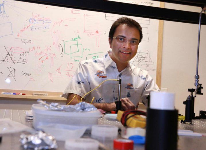
Electrical and computer engineering associate professor Rajesh Menon. Image: Dan Hixson/University of Utah College of Engineering
A type of invisibility cloak has been developed that could dramatically reduce the size of processing chips in future computers.
Photonics is the future of computing. Yet to be perfected, this form of physics is destined to play a central role in tomorrow’s data centres, mobile devices and pretty much everything that will connect the world.
The reason it will dominate is that despite not yet being an ideal way of transferring memory or energy in a manner that suits our current technologies, physicists know they’re on to something.
If only they could find a way to harness their current findings into anything tangible, manageable and ultimately, useable.

The main problem is at a small scale. Photonic chips are the holy grail, replacing today’s silicon-based variants with much faster options that consume less power and, thus, heat up less.
The photonics contained in these future chips could make up billions of devices, each with their own role, much like modern transistors. However unlike transistors, photonic devices don’t work well when they’re bundled beside each other.
They will not work because the light leakage between them will cause “crosstalk”, similar to radio interference. If they are spaced far apart to solve this problem, you end up with a chip that is much too large.
But University of Utah electrical and computer engineering associate professor, Rajesh Menon, and his team have developed a cloaking device to solve that problem.
“The principle we are using is similar to that of the Harry Potter invisibility cloak,” Menon said in a paper published in Nature Communications.
“Any light that comes to one device is redirected back, as if to mimic the situation of not having a neighbouring device.
“It’s like a barrier – it pushes the light back into the original device. It is being fooled into thinking there is nothing on the other side.”
Menon believes the most immediate application for this technology, and for photonic chips in general, will be for data centres similar to the ones used by services like Google and Facebook.
“By going from electronics to photonics, we can make computers much more efficient and ultimately, make a big impact on carbon emissions and energy usage for all kinds of things,” Menon said. “It’s a big impact and a lot of people are trying to solve it.”
A few months ago, a team of researchers took the first step towards a quantum internet, after they successfully teleported a particle of light 6km away over a straight line distance.
Having been teleported via a fibre optic cable across the city of Calgary, this teleportation has set a new record for transferring a quantum state by teleportation.
Soon after, researchers at Pennsylvania State University developed a very sophisticated, high-speed beam-scanning technique that could take printing speeds into overdrive.
By using a space charge-controlled KTN beam deflector – a kind of crystal made of potassium tantalate and potassium niobate – with a large electro-optic effect, the team has been able to increase the speed of 2D and 3D printing by up to 1,000.