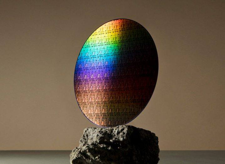
A VTFET chip wafer. Image: IBM
The chip developed by IBM and Samsung could be the next big leap in semiconductor efficiency.
A revolutionary breakthrough in chip design by IBM and Samsung could see phones last longer than a week without charging and crypto mining consume significantly less energy, ushering in a new generation of semiconductor efficiency.
Incorporating an unconventional and novel approach to chip design that uses a new vertical transistor architecture, the semiconductor technology has the potential to reduce energy usage by 85pc compared to existing fin field-effect transistors (finFET).
Most advanced semiconductors today have transistors stacked on them lying flat on the surface, with current flowing sideways. This new redesign will see transistors stacked vertically on semiconductors, allowing for more transistors to be stacked into a fixed space.
IBM and Samsung expect this new design, dubbed Vertical Transport Field Effect Transistors (VTFET), to allow for a long-anticipated continuation of Moore’s Law – the principle that the number of transistors incorporated in a densely populated chip will double every two years.
Because there is a finite space to fill, engineers have been running out of space as more and more transistors are being crammed together to make chips more efficient and powerful. The new VTFET design, announced last month, gives the industry fresh hope as it grapples with a global chip shortage.
Mukesh Khare, vice-president of hybrid cloud and systems at IBM Research, said the announcement is about “challenging convention and rethinking how we continue to advance society and deliver new innovations that improve life, business and reduce our environmental impact.”
VTFET has the potential to do one of two things at a time: it can either reduce energy consumption by 85pc or double its performance. This makes it even more advanced than the recently announced nanosheet technology that fits up to 50bn transistors in the space of a fingernail.
Another potential revolutionary outcome of VTFET is that data encryption will require significantly less energy and have a smaller carbon footprint. IoT devices will also have lower energy needs, allowing them to operate in diverse environments such as ocean buoys, autonomous cars and even spacecraft.
The collaborative research between IBM and Samsung took place in the Albany Nanotech Complex at the SUNY Polytechnic Institute in New York. Once ready, the VTFET chips will be manufactured by Samsung and used in IBM’s own server platforms.
Don’t miss out on the knowledge you need to succeed. Sign up for the Daily Brief, Silicon Republic’s digest of need-to-know sci-tech news.