

Future glasses that could benefit from smaller electronics. Image: Syda Productions/Shutterstock
A team of researchers from Queen’s University Belfast has found a way of making our electronic devices even smaller, without needing to use graphene.
In our bid to make smaller and smaller electronics for devices, both at a consumer level and within the internet of things (IoT), researchers are constantly trying to make elements – such as electrical conducing sheets – thinner.
One such breakthrough has just been announced by Queen’s University Belfast (QUB), which has discovered a way to transform these sheets to a thinner version, measuring just a few atoms in thickness.

While many other innovations in recent months and years have involved graphene, the team’s creation is still 2D, but slightly thicker.
However, despite this increased thickness, it can do something that graphene can’t: it can appear, disappear or move around within the crystal, without permanently altering the crystal itself.
This means that one day in the future, even smaller electronic devices could be created, as electronic circuits could constantly reconfigure themselves to perform a number of tasks, rather than just having a sole function.
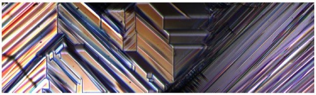
The domain walls found in the material. Image: QUB
Being able to ‘etch a sketch’ electronics
According to Prof Marty Gregg of QUB, such breakthroughs offer profound improvements within many aspects of modern and future life, from microelectronic devices to healthcare.
“Our research suggests the possibility to ‘etch a sketch’ nanoscale electrical connections, where patterns of electrically conducting wires can be drawn and then wiped away again as often as required,” he explained.
“In this way, complete electronic circuits could be created and then dynamically reconfigured when needed to carry out a different role, overturning the paradigm that electronic circuits need be fixed components of hardware, typically designed with a dedicated purpose in mind.”
Achieving this has been no easy feat, as two major hurdles exist to making these sheets viable.
The first is figuring out how to mimic the conductive behaviour of metallic wires using long straight walls of the 2D material.
The second is to figure out exactly where and when the walls appear, and how to reposition or delete them.
Thankfully, the team found that such sheets can be created by squeezing the crystal at precisely the location they are required, using a targeted acupuncture-like approach with a sharp needle.
Earlier this month, another QUB team announced the development of a new ‘wonder material’, which it claimed could spell the end of cracked phone screens.


